Packaging Systems
Advanced Packaging Solutions
Custom BEOL package solutions spanning design through assembly and test, supporting PoP and SiP modules across IoT, mobile, optical, high-speed, memory, and industrial applications.
Request a Quote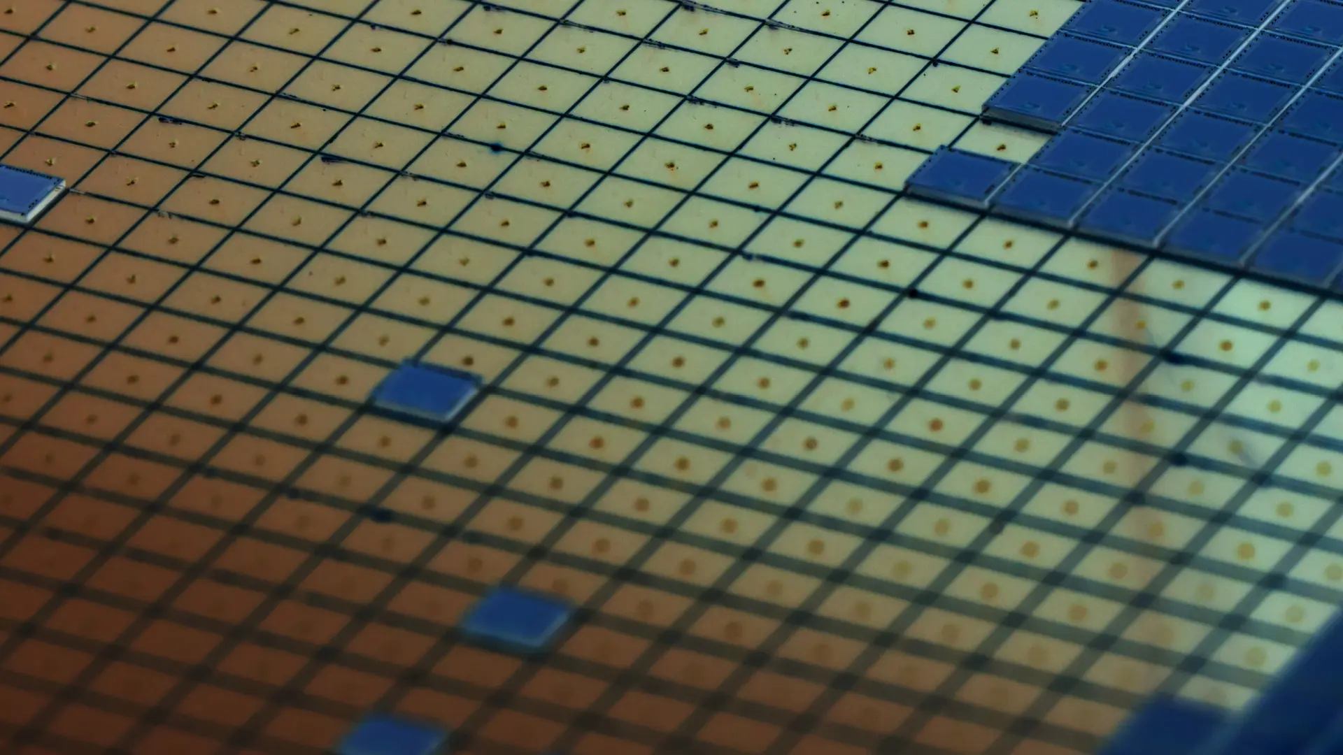

What We Offer
Turn-Key Package Design
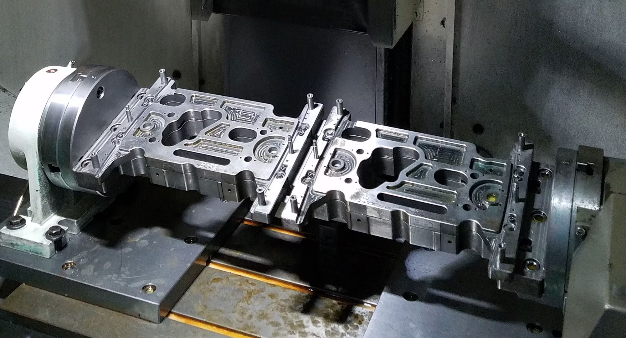
Wafer-Processing
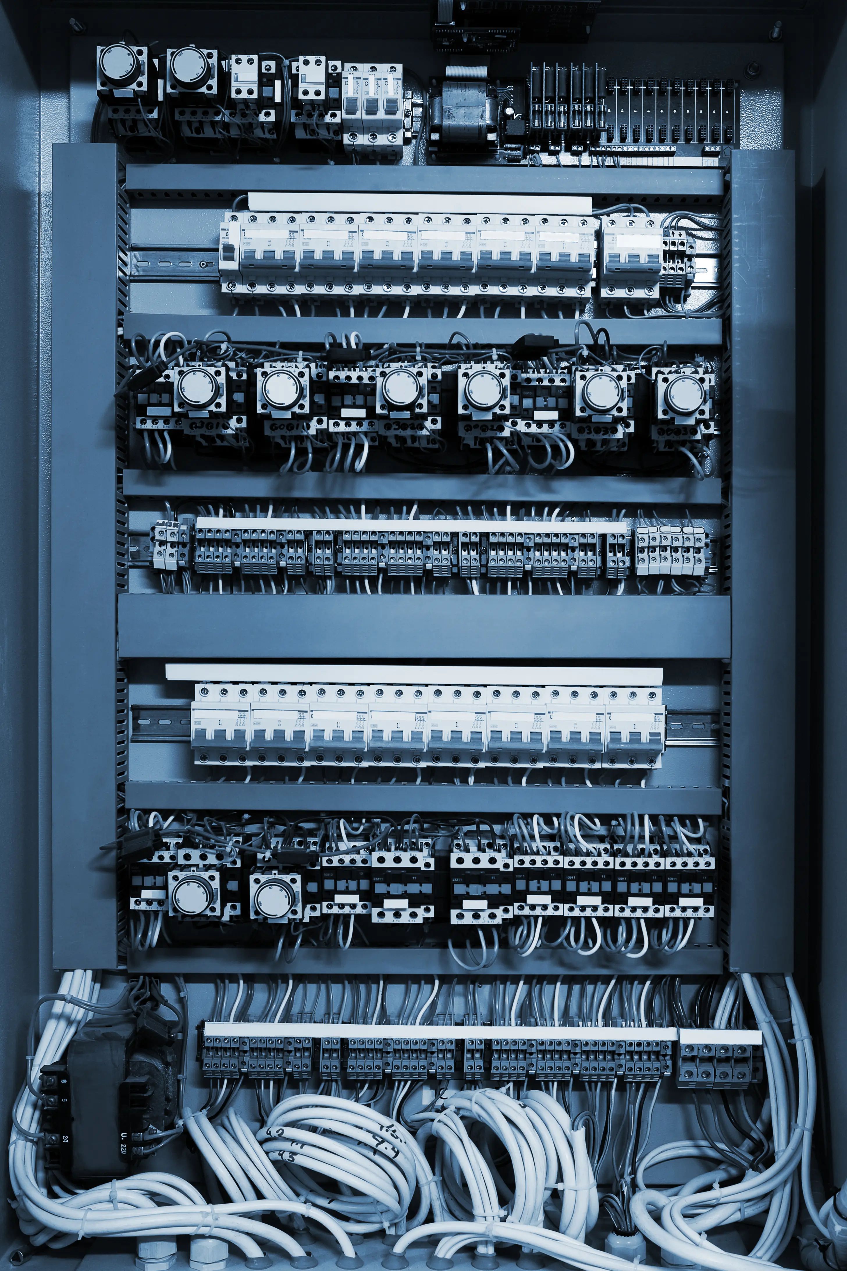
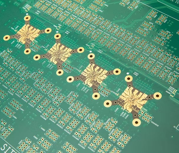
Substrate Fabrication
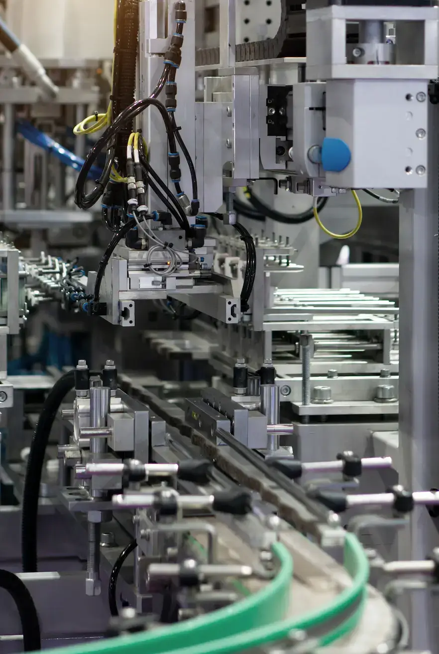
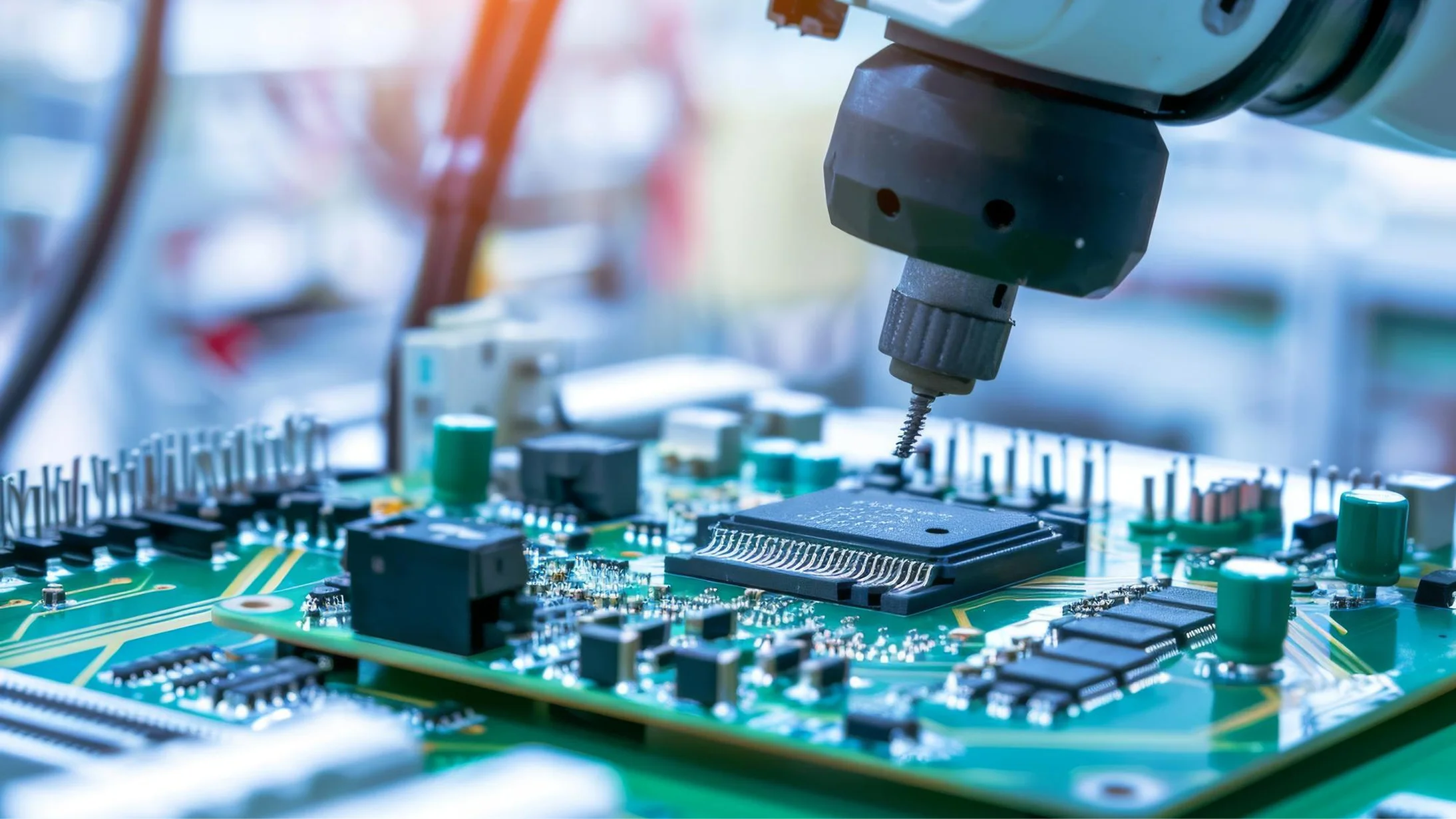
Package Assembly
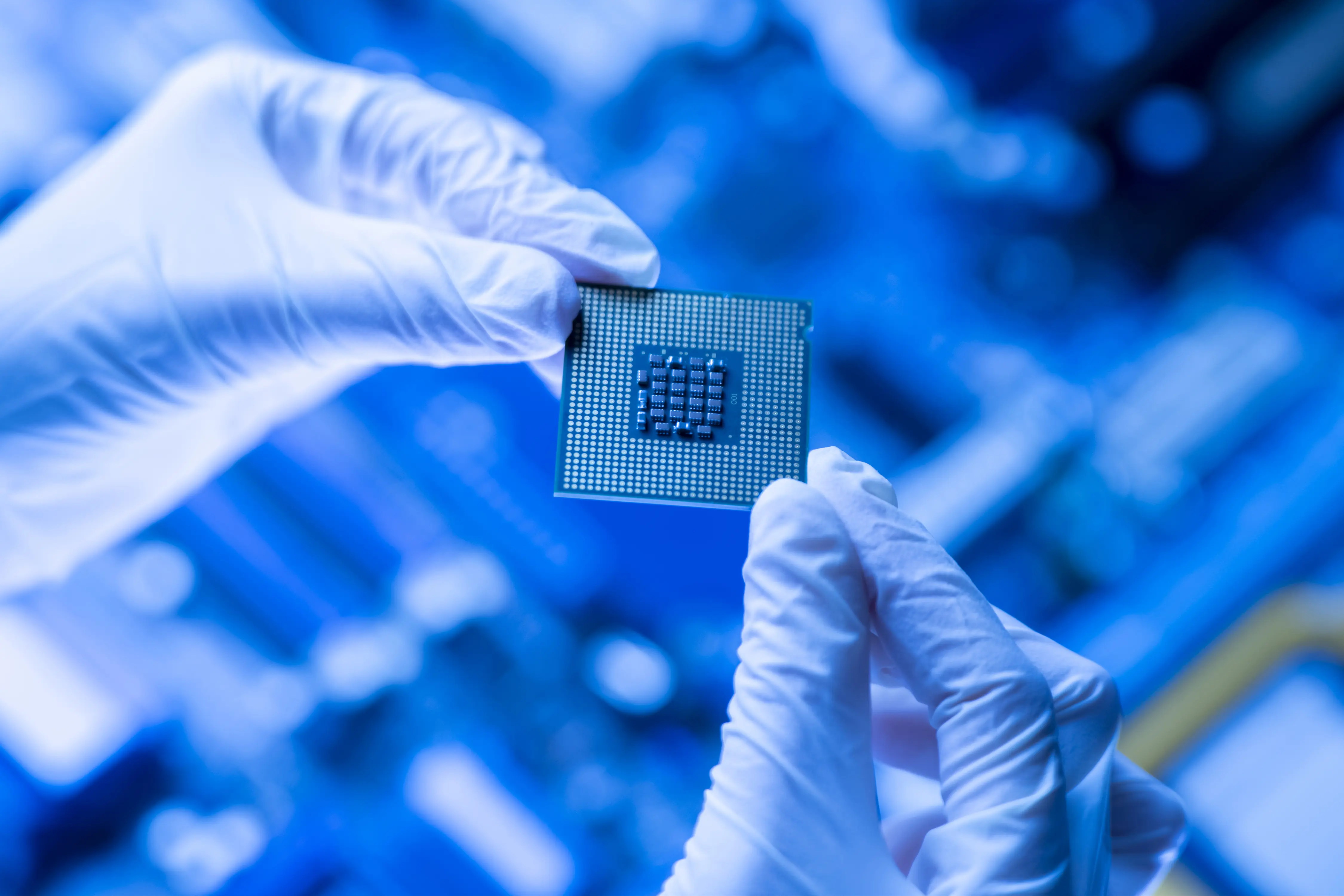
2.5D/ 3.0D Chiplet
Capabilities
PalPilot enables customer specific Back End of Line (BEOL) Packaging System solutions & services.
- Design Service: Substrate & Packaging
- SI/PI Modeling
- Wafer Process: Cu Pillar Plating, Grinding Dicing
- Substrate Fabrication: FCBGA (Small & High Volume)
- Package Assembly: 40um Flip Chip Pitch
- Advanced Packing System: TSV + Multi Layer RDL
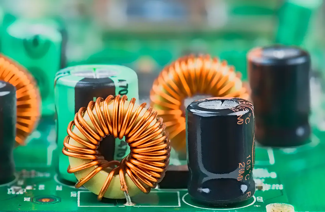
Substrate Solutions
PalPilot’s substrate division delivers full interconnect solutions from SI/PI modeling, interconnect routing & fabrication.
-
Full Package Modeling & Design Service
-
5 & 7 Day BGA/CSP Quick Turn Fabrication
-
Ultra-Thin “Coreless” Package Structures
-
Ceramic On Organic Laminate (COOL) Package Product Launch
-
Full Package SiP Product Solutions
Package System Design
Custom Package System design including substrate selection/routing, package assembly structure definition (PoP, SiP, single die, etc.) meeting industry specific DFM & reliability requirements (Deliverables: 2D DXF & Various Design Files).
Signal/Power Integrity Modeling
PCB & Package system, passive interconnect, electrical signal & power modeling (Deliverables: SI/PI Report & Program Files).
Industry Focused Package Systems Integration
B2B Package Systems, technology & supply program management/development from NPI, production ramp, to high volume manufacturing of high power, high speed package systems showing calculated improvement of customer’s corporate ROA components
(Deliverable: A calculated improvement of customers ROA components including impact on Revenue, SG&A, COGS, Fix/Current Asset).

Thinking globally. Acting locally.
PalPilot enables application-specific semiconductor packaging solutions backed by global manufacturing capabilities and strict quality standards. Our team supports customers from design through production to deliver reliable, scalable technologies.
Talk to an ExpertRelated Industries


Browse Related Products


FAQs
PalPilot delivers customer-specific BEOL (Back End of Line) packaging system solutions, covering design, wafer processing, substrate fabrication, package assembly, and test
Yes. PalPilot provides turn-key package design, including substrate and package design, SI/PI modeling, and full system definition to ensure performance and manufacturability
We support advanced packaging systems, including 2.5D / 3.0D chiplet packaging, TSV integration, and multi-layer RDL architectures for high-performance applications
Our capabilities include wafer processing, Cu pillar plating, grinding and dicing, and Au or Cu bumping for flip-chip applications
PalPilot supports FCBGA substrate fabrication for both small and high-volume production, with fine features such as 15µm line/space, TSV ~1.0µm, and multi-layer RDL.
We support package assembly with fine-pitch flip-chip, including 40µm flip-chip pitch, plated circuitry, molding compounds, and optional solder mask processes.
Our packaging systems support wearable/IoT, mobile, optical/VCSEL, high-speed/wide-bandwidth, memory, and advanced thermal applications, serving automotive, medical, communications, consumer, and industrial markets.
Build What’s Next
From first prototypes to high-volume production, our engineers are ready to guide your project forward.
Request a Quote