PCB Design/Layout
PCB Design Built for Production
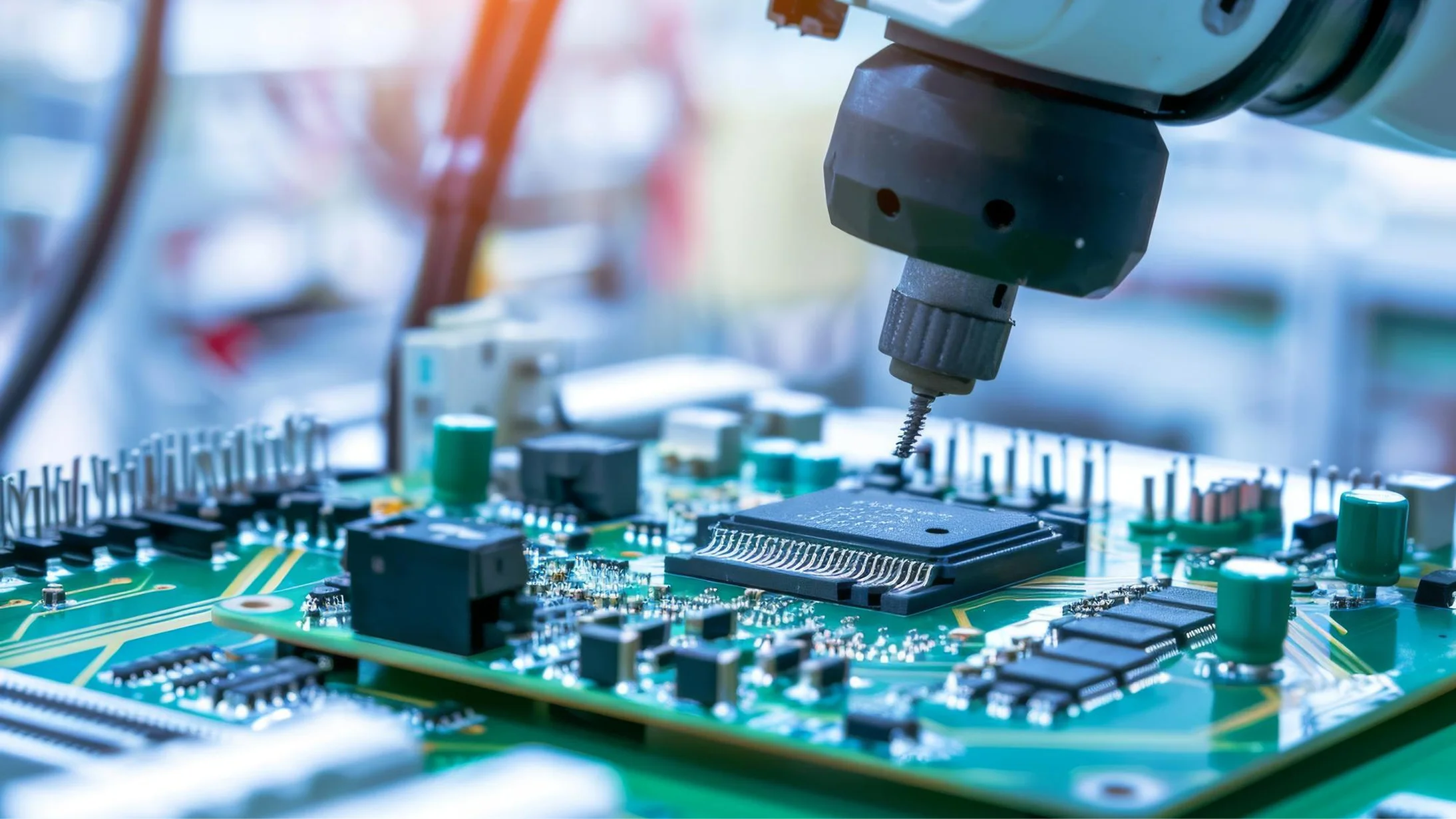
Our PCB layout services combine precision engineering with real-world manufacturing expertise. From stack-up development and controlled impedance routing to DFM optimization, we design boards that are not only functional, but scalable, reliable, and production-ready.
Request a Quote

What We Offer
Full Project Design
Library Service
Around-the-Clock Routing
Library and Routing Studies
Constraint Manager
Design Partitioning
Pre-Fab DFM Validation
Design Platforms


Capabilities
Experienced Technologies
-
DDRx, LPDDRx, GDDRx
-
PCIe Gen 3, Gen 4, Gen 5
-
SAS-3, SAS-4
-
Infiniband
-
1Gb and 10Gb Ethernet
-
Thunderbolt 2, Thunderbolt 3
-
SFP28, QSFP28
-
FPGA, DSP, Programmable SoCs
Advanced PCB Design
- Multilayer PCB designs for compact and high-density applications
-
Fine-pitch components including BGAs, QFNs, and CSPs
-
Stack-up definition with material selection based on electrical and thermal needs
-
Component placement optimized for routing efficiency and assembly yield
-
Board designs tailored for both prototype and volume production
High-Speed & Mixed-Signal Design
-
Controlled impedance routing for high-speed signal paths
-
Layout support for common high-speed interfaces and buses
-
Mixed-signal partitioning to isolate noise-sensitive analog circuits
-
Power distribution network (PDN) planning and decoupling strategies
-
EMI-aware routing, grounding, and return-path control
DFM-Driven Design
-
Early DFM reviews aligned with fabrication and assembly constraints
-
Via structures, trace widths, and spacing selected for manufacturability
-
Panelization and fiducial considerations built into the layout
-
Assembly-friendly footprint and land-pattern optimization
-
Design decisions made to balance cost, yield, and reliability

Thinking globally. Acting locally.
With a global mindset and coordinated organization, supported by local teams managing your product lifecycle every day, PalPilot enables highly complex and technologically advanced projects.
Our global footprint and deep expertise provide innovative manufacturing and supply-chain solutions, built on standardized processes and a unified culture. This allows us to scale with your needs while maintaining the proximity and responsiveness required to support your business at every stage.
Talk to an ExpertApplications


Browse Related Products


FAQs
To begin a PCB design, we typically require:
-
Schematic diagrams (if available)
-
Bill of Materials (BOM)
-
Mechanical drawings or enclosure constraints
-
Target specifications (voltage, current, frequency, environment)
-
Compliance requirements (UL, IPC class, etc.)
If you don’t have everything finalized, our engineering team can assist with schematic capture and DFM review to move your project forward.
Yes. PalPilot provides:
-
Full schematic capture
-
Multi-layer PCB layout
-
High-speed layout design
-
RF and impedance-controlled routing
-
HDI and fine-pitch component layout
-
Rigid-flex and flex PCB design
Our engineers design with manufacturability in mind to reduce iterations and improve yield.
Absolutely. We specialize in:
-
Controlled impedance stack-up design
-
Differential pair routing
-
Signal integrity (SI) considerations
-
Power integrity (PI) optimization
-
EMI/EMC-aware layout practices
We work closely with fabrication teams to ensure stack-up accuracy and performance reliability.
Every design goes through:
-
DFM (Design for Manufacturability) review
-
DFT (Design for Testability) review
-
Panelization planning
-
Fabrication capability alignment
-
Assembly feasibility checks
Designs are optimized early to reduce cost and lead time.
Yes, we provide a complete path from:
-
PCB design
-
Prototype fabrication
-
Assembly (SMT, through-hole, mixed technology)
-
Testing and validation
-
Full production scaling
This integrated approach reduces handoff risk and accelerates time-to-market.
Build What’s Next
From first prototypes to high-volume production, our engineers are ready to guide your project forward.
Request a Quote