PCB Layout Decisions That Impact Signal Integrity
Jun 02, 2026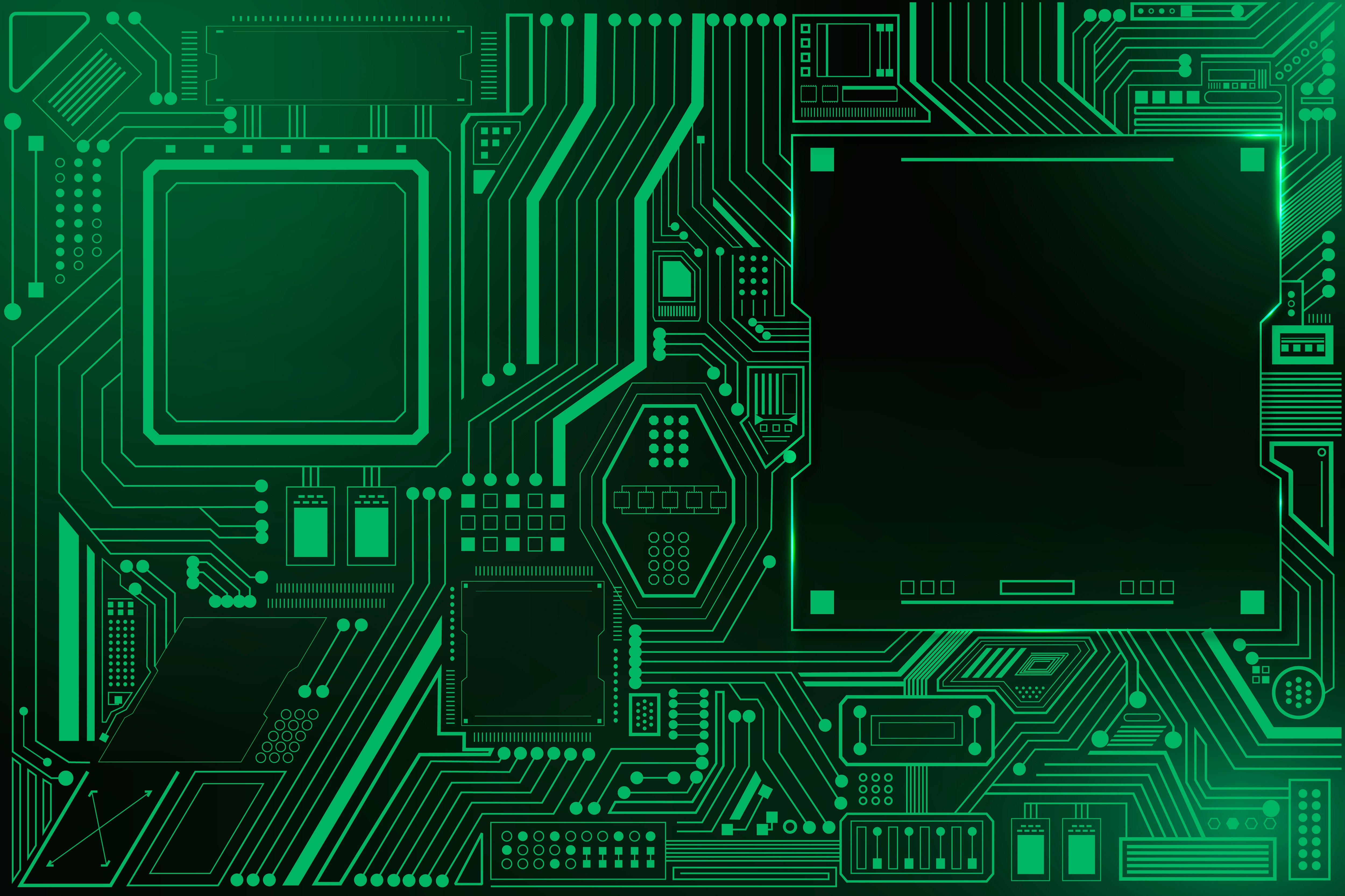
As PCB designs continue moving toward higher speeds and greater density, signal integrity has become a critical part of the layout process. Even electrically correct schematics can experience performance problems if PCB routing, stackup structure, and return path planning are not properly considered during layout.
Many signal integrity issues are not caused by component failure, but by layout decisions that introduce noise, reflections, impedance discontinuities, or timing instability into the system.
Below are some of the most common PCB layout decisions that impact signal integrity in
high-speed designs.
1. Poor Return Path Planning
One of the most common signal integrity issues in PCB layout is an improperly managed return current path.
High-speed signals naturally follow the path of least impedance, typically returning underneath the signal trace along the reference plane. When return paths are interrupted by:
- split planes
- gaps in reference layers
- poorly planned layer transitions
- excessive reference discontinuities
current flow becomes less predictable and EMI risk increases.
A common issue in multilayer PCB layouts is routing high-speed signals across split ground regions, forcing return currents to detour around plane discontinuities. This increases loop inductance and can create additional radiated emissions during system validation.
Maintaining continuous reference planes throughout critical routing paths helps improve signal stability and reduce EMI-related issues later in development.
2. Improper Differential Pair Routing
Differential pair routing plays a major role in high-speed communication interfaces such as:
- USB
- PCIe
- Ethernet
- LVDS
- DDR interfaces
Signal integrity problems can occur when differential pairs experience:
- inconsistent spacing
- length mismatch
- excessive via transitions
- sharp routing discontinuities
- inconsistent reference environments
These issues may introduce:
- skew
- impedance imbalance
- degraded timing margin
- increased common-mode noise
One common layout challenge occurs near dense BGA fanout regions, where routing
constraints can unintentionally create asymmetrical differential pair geometries.
Maintaining consistent pair spacing, reference planes, and routing structure throughout the signal path helps improve timing consistency and high-speed performance.
3. Inadequate Stackup Planning
PCB stackup design has a direct impact on:
- impedance control
- crosstalk behavior
- EMI performance
- return path continuity
- routing efficiency
Poor stackup planning can create unstable impedance environments and increase noise
sensitivity throughout the system.
A common issue in high-speed PCB layouts is developing stackups primarily around layer count rather than electrical performance requirements. This can create routing compromises later in the design cycle.
High-speed layouts typically benefit from:
- solid reference planes
- tightly coupled signal layers
- controlled dielectric spacing
- balanced copper distribution
- predictable impedance structures
Early collaboration between PCB layout and fabrication teams helps improve both signal
integrity performance and manufacturability.
4. Excessive Via Usage in High-Speed Signals
Vias introduce impedance discontinuities and parasitic inductance into high-speed signal paths.
While vias are unavoidable in many complex PCB designs, excessive layer transitions can
negatively impact:
- insertion loss
- signal reflections
- timing consistency
- high-frequency performance
This becomes increasingly important in:
- PCIe routing
- DDR memory layouts
- RF designs
- dense BGA escape routing
One common issue in high-speed layouts is unnecessary via transitions introduced during
late-stage routing cleanup, particularly in congested areas near processors or high-pin-count devices.
Reducing unnecessary layer transitions and maintaining cleaner signal paths helps minimize signal degradation and improves overall routing consistency.
5. Poor Decoupling Capacitor Placement
Power integrity and signal integrity are closely connected in modern PCB designs.
Improper decoupling placement can increase:
- voltage ripple
- transient instability
- switching noise
- power distribution noise
A common issue occurs when decoupling capacitors are placed too far from IC power pins,
increasing loop inductance between the capacitor and device.
In high-speed systems, effective decoupling requires:
- short current return paths
- low-inductance placement
- proper capacitor distribution across power rails
- strong grounding continuity
Insufficient decoupling strategy can contribute to signal instability, EMI problems, and
inconsistent system behavior during validation testing.
Final Thoughts
Signal integrity is heavily influenced by PCB layout decisions made early in the design process. Even relatively small routing, grounding, or stackup decisions can significantly impact system stability, EMI performance, and long-term reliability.
As high-speed PCB designs continue becoming more complex, close collaboration between
layout, signal integrity, and manufacturing teams becomes increasingly important for achieving stable production-ready designs.
At PalPilot, our engineering and manufacturing teams work closely with customers to support PCB layout, stackup planning, DFM review, and production requirements throughout the product development cycle.
Need support for your next PCB design project? Contact PalPilot to discuss your design and manufacturing requirements.
Request a Quote
Have a design, schematic, or idea? PalPilot’s expert team will help turn it into reality with precision and speed. Share your project details, and we’ll provide a competitive quote with the fastest lead time possible.
"*" indicates required fields
Related Articles
How to Choose the Right PCB Manufacturer (Avoid These 5 Costly Mistakes)
Choosing the wrong PCB manufacturer can lead to delays, quality issues, and hidd... Read More
When Does Custom Magnetics Make Sense?
Read More
Top 10 Design Considerations for PCB Manufacturability and Reliability
Designing a good Printed Circuit Board (PCB) takes more than selecting drills an... Read More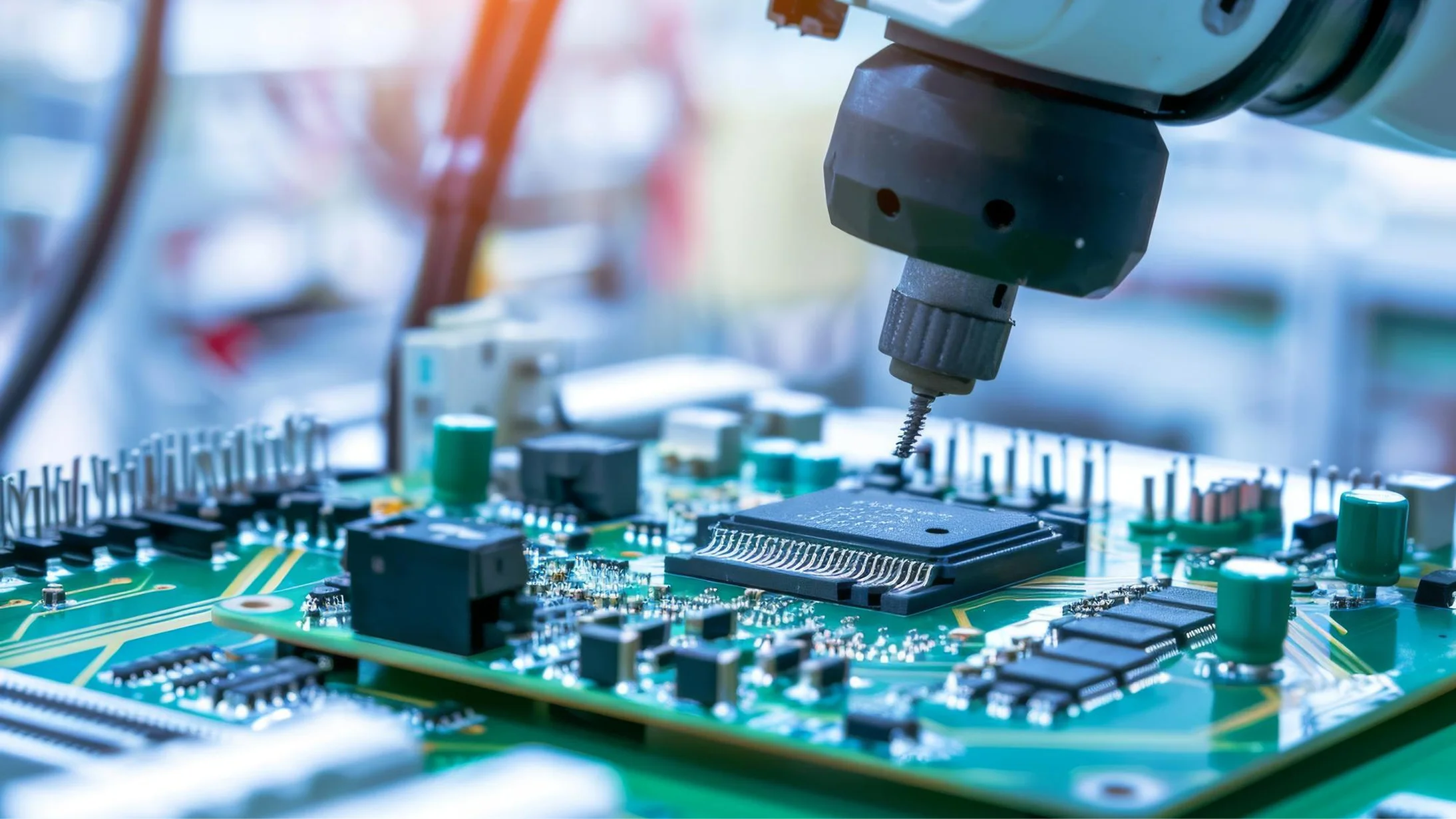
Build What’s Next
From first prototypes to high-volume production, our engineers are ready to guide your project forward.
Request a Quote